|
|
|
|
|
|
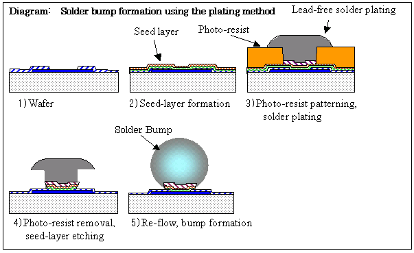
Fujitsu Achieves Breakthrough in Ultrafine-Pitch Solder Bumping and Flip-Chip BondingTokyo, December 15, 2003 -- Fujitsu Limited today announced that it has developed new technology that enables formation of ultrafine pitch 35 micron (center-to-center distance of bumps) solder bumps (*1), and high-precision flip-chip bonding (*2) interconnection. This breakthrough technology increases connection density by approximately 50 times compared to conventional flip chip interconnections and actualizes downsizing of LSIs and LSI packaging. BackgroundWith the continuing strive toward downsizing and higher functionality of a variety of devices such as mobile phones and digital cameras, demand is increasing for both finer bump pitch and high-precision interconnection technologies, which enable downscaling of LSIs and LSI packaging. Flip-chip bonding, which is widely utilized as ideal for reducing the mounting area of LSIs and LSI packaging, entails interconnection of molten solder bumps. In order to avoid short-circuiting between solder bumps, currently bump pitches are in general between about 200 micron to 250 micron. To enable further downsizing of LSIs and LSI packaging, both finer pitch solder bumping and high-precision flip-chip bonding capable of avoiding short-circuiting between solder bumps are indispensable. Fujitsu's New TechnologiesFujitsu has succeeded in developing the world's first-ever ultrafine-pitch solder bumping technology with 35 micron pitch, and high-precision flip-chip bonding technology that ensures interconnections. Features of the new technologies are as follows: 1. Ultrafine-pitch solder bumping technology This new technology adopts solder bump formation using a plating method (*3). To narrow down the bump pitch, it is necessary to refine the photo-resist resolution used for bump formation, raise the bump height, and have even formation. However in the past, the smaller the bump pitch became, the more increasingly difficult it was to have even formation of bumps, due to the fact that the plating solution did not sufficiently reach photo-resist openings. This resulted in uneven bump formation. With Fujitsu's new technology, by improving the photo-resist material, optimizing the parameters for exposure and developing of photo-resist patterns, and precisely controlling the electric current used during plating, the even formation of ultrafine-pitch bumps with height is now possible. Furthermore, as part of Fujitsu's eco-friendly mission, lead-free solder bumps have been used. 2. High-precision flip-chip bonding technology With conventional flip-chip bonding, by heating the bumps while a calibrated force is applied to them, the bumps are melted and then pressure-welded. However, with ultrafine-pitch bumps, short-circuiting frequently occurred when this method was employed due to neighboring bumps coming into contact with each other. Furthermore, in order to ensure connection to the connection surface, a unique process to mechanically planarize bumps was necessary to eliminate any bump height deviations. With Fujitsu's new technology, by employing precision-control of temperature and force during flip-chip bonding, high-precision flip-chip bonding is now possible without the need to employ a bump planarization process. Through these new techniques, short-circuiting can be avoided and connections can be ensured even during flip-chip bonding of LSIs with ultrafine-pitch solder bumps in area-array configuration. Utilizing this technology, Fujitsu has begun to supply to Value Added Technologies (VATECH) (*5) of South Korea a chip-on-chip Multi-Chip Module (MCM) (*4), consisting of 4 units of detection signal-processing CMOS devices for which the entire connection surface is covered with 160,000 ultrafine-pitch solder bumps in full area-array configuration, that have been flip-chip bonded to an X-ray detection device. VATECH has succeeded in installing this chip-on-chip MCM and verifying operation of a dental X-ray image sensor. The chip-on-chip MCM for the dental X-ray imaging sensor has been manufactured by Fujitsu Integrated Microtechnology Ltd. with assistance from Fujitsu Laboratories Ltd. Future DevelopmentsIn order to meet demands for further miniaturization and higher functionality of mobile devices and others, Fujitsu is committed to the continued development of downscaled LSIs and LSI packaging utilizing this new technology. Fujitsu is also exploring the applicability of this technology for stud bumps (*6) and gold bumps (*7), which were not alternatives with conventional solder bump pitches.Notes
About Fujitsu
All company/product names mentioned may be trademarks or registered trademarks of their respective holders and are used for identification purpose only. |
|
|