|
|
Fujitsu Laboratories Ltd.
Fujitsu Limited
|
Fujitsu Develops High-Speed Multichannel Optical Switch Based on MEMS Mirrors
-- World's Fastest Switch Provides Key to Next-Generation Optical Networks --
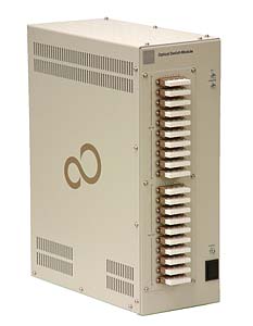
Tokyo, September 29, 2003 -- Fujitsu Laboratories Ltd. and Fujitsu Limited today announced the development of an 80-channel optical communications switch that adopts MEMS (micro electro-mechanical system*1) mirrors (see figure 1). The new device achieves a switching speed of one millisecond, the fastest of any multi-channel optical switch to date.
The new switch is expected to enable the development of the optical cross-connect systems essential for next-generation optical transmission networks.
Details of the technology used in this switch were presented at ECOC-IOOC 2003 (European Conference on Optical Communication/International Conference on Integrated Optics and Optical Fibre Communication), held in Rimini, Italy starting September 21.
Background
Because of the need to efficiently transmit the massive amounts of data carried over high-speed Internet connections, there has been an increase in demand for cross-connect equipment, which is required for the effective operation of fiber-optic networks and for network interconnections. With conventional equipment, however, optical signals need to be converted to electrical signals for processing, limiting the ultimate performance that could be achieved through wave-division multiplexing or other optical multiplexing techniques. The goal, therefore, has been to develop cross-connect equipment with all-optical switching so that the optical signals need not be converted.
About the Technology
Fujitsu's development depends on MEMS mirrors to bounce light beams. MEMS mirrors can be tilted to deflect the beam to different points in space, resulting, in this case, in a three-dimensional optical MEMS-mirror switch. The key features of this technology are as follows:
- Rapid switching
A notch filter (*2) in the MEMS mirror serves to suppress the mechanical resonance (*3) that normally occurs when switching the optical signal. The notch filter eliminates just the MEMS mirror's resonant frequency from the driving electrical waveform. The use of this control technology and a special comb-driven rapid-response MEMS mirror array (*4) developed by Fujitsu enables faster switching times.
- Compact optical switching fabric
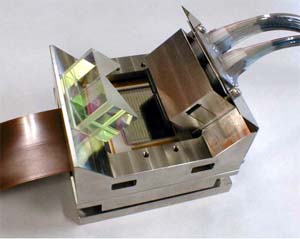
Fujitsu developed a folded optical switch fabric configuration whereby the input beam is reflected through a roof-type retro-reflector on its way to the output (see figure 2). Compared to flat mirrors, this configuration halves the length of the optical path, making for a more compact switch overall.
- Optic power-level feedback mechanism
The tilt of the MEMS mirrors is precisely controlled thanks to a feedback loop in a built-in control function, which maintains the optical power at a fixed level. This makes it possible to compensate for variations in the power levels of each channel and also eliminates the need to have variable optical attenuators external to the switch.
The combination of these technologies results in a switch with 1 millisecond switching speed, compact dimensions (150 x 400 x 300 mm) and optical power stability within ±0.5 dB.
Some of this research was conducted on behalf of the Telecommunications Advancement Organization of Japan under a contract for the research and development of photonic networking using optical burst switching.
Glossary
- MEMS (Micro electro-mechanical systems)
Devices that integrate electrical circuitry and mechanical structures. Also called "micro-machines."
- Notch filter
A filter that eliminates a specified narrow bandwidth frequency from a signal consisting of frequencies of a given bandwidth.
- Mechanical resonance
A phenomenon whereby the input of an external signal at a certain frequency induces strong vibrations.
- Comb-driven MEMS mirror array
Use of a comb-shaped electrode structure to drive the MEMS mirrors results in greater driving power than with a planar structure.
About Fujitsu Laboratories Ltd.
Founded in 1968 as a wholly owned subsidiary of Fujitsu Limited, Fujitsu Laboratories Limited is one of the premier research centers in the world. With a global network of laboratories in Japan, China, the United States and Europe, the organization conducts a wide range of basic and applied research in the areas of Multimedia, Personal Systems, Networks, Peripherals, Advanced Materials and Electronic Devices.
Internet: http://www.labs.fujitsu.com/.
About Fujitsu
Fujitsu is a leading provider of customer-focused IT and communications solutions for the global marketplace. Pace-setting technologies, highly reliable computing and telecommunications platforms, and a worldwide corps of systems and services experts uniquely position Fujitsu to deliver comprehensive solutions that open up infinite possibilities for its customers' success. Headquartered in Tokyo, Fujitsu Limited (TSE:6702) reported consolidated revenues of 4.6 trillion yen (US$38 billion) for the fiscal year ended March 31, 2003. For more information, please see : http://www.fujitsu.com/.
All company/product names mentioned may be trademarks or registered trademarks of their respective holders and are used for identification purpose only.
Please understand that product prices, specifications and other details are current on the day of issue of the press release, however, may change thereafter without notice.
|
|