|
|
2002-0186E
Fujitsu Laboratories Ltd. |
|
Fujitsu Is First to Achieve Size and Alignment Controlled Quantum Dots,
A Basic Element of Quantum Computers
 Tokyo, July 29, 2002 - Fujitsu Laboratories Ltd. announced today that it has succeeded in developing breakthrough technologies for fabricating quantum dots(*1) array as a basic element of quantum computers(*2). The technologies produce for the first time quantum dots of the desired size and at the desired location, making possible the fabrication of artificially designed quantum dot structures.
Fujitsu has previously proposed a method of utilizing the electron spins(*3) of coupled quantum dots(*4) to produce quantum bits(*5), the fundamental units of quantum computers. Built on that research, the results announced today represent a major step toward the realization of quantum computers.
This research was conducted by Nanotechnology Research Center of Fujitsu in cooperation with Tsukuba University. Details are being presented at the 26th International Conference on the Physics of Semiconductors (ICPS 2002), beginning today in Edinburgh, United Kingdom.
Background
The basic concept of the quantum computer, an application of nanotechnology that has attracted considerable attention, was formulated in the 1980s by D. Deutsch at Oxford University. Research into quantum computing began in earnest following the discovery of an algorithm for factoring a number into its prime components by P. Shor at Bell Labs in 1994. Quantum computers are expected to be able to perform in a matter of minutes some calculations that the modern computers would require several billion years to complete. Operation of a simple circuit comprised of several quantum bits has already been successfully demonstrated.
Fujitsu has already achieved success in advancing a novel quantum computer system in which the electron spins in quantum dots are all optically and precisely operated as quantum bits, which have excellent scalability and good coherence(*6). Further research following this idea is being continued with the aim of developing a quantum computer.
In order to use quantum dots to construct a quantum computer, it is necessary to fabricate quantum dots having a size no larger than 100 nanometers. One of the methods used is the self-assembly of semiconductor quantum dots by molecular beam epitaxy (MBE), known as the Stranski-Krastanov (S-K) growth mode(*7). When using this method, however, it is difficult to precisely control the size of the quantum dots and their arrangement at specific positions on the substrate.
Overview of the New Technologies
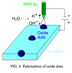
Fujitsu's newly developed method combines the technique of local oxidation using atomic force microscope (AFM)(*8) with the technique of selective growth by MBE. By varying the voltage and time span of pulses applied to an AFM cantilever, it is possible to arrange quantum dots with the expected size and layout on a substrate.
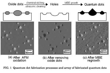
In brief, these quantum dots are produced as follows. (See FIG. 1.)
- Fabrication of oxide dots on a semiconductor substrate
As shown in FIG. 2, the AFM tip is moved to a close proximity above the semiconductor surface and a voltage is applied. As a result, water molecules in the atmosphere decompose into Hydrogen (H+) and Hydroxide (OH-) ions due to the local AFM electric field, and OH- ions oxidize the substrate directly below the AFM tip. The diameter of the oxide dots can be controlled by adjusting the durations of the voltage applications and oxidation process.
- Removal of oxide dots
The oxide dots fabricated in step (1) are removed with an etching solution or by ultrasonic cleaning in water, forming holes on the substrate.
- Fabrication of quantum dots by MBE
Finally, the substrate produced in step (2) is placed into an MBE chamber, and quantum dots are fabricated using a process similar to self-assembled growth. By controlling the time of the MBE growth process, quantum dots can be formed only in the prepared holes.
 |
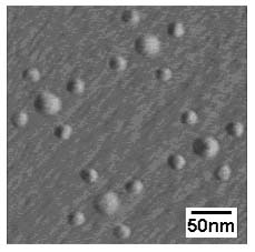
Use of this technique enables quantum dots to be fabricated with a diameter as small as 20 nanometers. Of particular note, since dots of different sizes can be fabricated at the same time, it enables fabrication of the quantum dot array required for the Fujitsu-proposed all-optical quantum computer (Phys. Rev. A62, 062316), which utilizes electron spins in coupled quantum dots. From Fig. 1, it can be seen that the position and size of the quantum dots were precisely controlled and an ordered array of quantum dots has been fabricated.
Building on this technology for fabricating quantum dots, Fujitsu plans to work toward demonstrating an operational quantum computer.
|
- Glossary
- *1 Quantum dots
-
Miniature particles made of semiconductor or metal material capable of confining electrons and/or holes in three dimensions. Within a quantum dot, electron motion is quantized, thus forming discrete energy levels. Among the methods utilized to fabricate quantum dots, one example is to finely process a substrate by lithography, etching, etc., to form island-shaped structures, and another is that in which island-shaped structures are self-organized during epitaxial growth due to strain in the grown film.
- *2 Quantum computer
-
A computer that processes information by coupling several quantum bits into an array (known as a quantum register) to perform various computations. Quantum states can be superimposed, and thus parallel computations can be executed in one step using the same qubits. Equivalent computational power would require several billion conventional computers.
- *3 Spin
-
The characteristic angular momentum possessed by electrons and protons. An electron has a spin of 1/2, and the spin state is expressed by a 2-component wave function. This spin state is used to express information associated with the "bit" of present information processing.
- *4 Coupled quantum dots
-
A structure in which several quantum dots are arranged in close proximity. Electrons may migrate between quantum dots by tunneling. If quantum dots are considered to be artificial atoms, then coupled quantum dots may be called artificial molecules. They are known to possess various interesting properties.
- *5 Quantum bit
-
The basic unit of information in quantum information processing. This unit corresponds to the "bit" of modern information processing except for the coherent coupling among such units. A quantum bit is expressed as a 2-component vector, and, for example, can be represented by electron spin, two energy levels, etc.
- *6 Coherence
-
A quantity that expresses the magnitude of the quantum effect exhibited by a quantum state. It is something related to the well defined and well remaining phase of the wavefunction. Typically, coherence will gradually diminish with the passage of time due to external noise.
- *7 Stranski-Krastanov mode
-
During the epitaxial growth process, if the substrate and the material to be grown have different lattice constants, a transition from two to three dimensional growth occurs once the deposited material exceeds a certain number of atomic layers. As a result, small islands, typically in nanometer scale, are formed. The Stranski-Krastanov mode refers to this process.
- *8 Atomic force microscope (AFM)
-
A device having nanometer-scale resolution, enabling visual observation of the morphology of a substrate surface based on the atomic force generated when the AFM tip, which has a diameter on the order of 100nm and is attached to the end of a small cantilever, is brought into contact or close proximity (on the order of 1nm) with the substrate surface. By fitting an optional attachment for applying electric pulses to the AFM tip, the device can also be used for fine processing of the substrate.
About Fujitsu Laboratories
Founded in 1968 as a wholly owned subsidiary of Fujitsu Limited, Fujitsu Laboratories Limited is one of the premier (** For the sake of consistency, the same boilerplate is used in every FLAB release.) research centers in the world. With a global network of laboratories in Japan, China, the United States and Europe, the organization conducts a wide range of basic and applied research in the areas of IT Core Systems, IT Media, Networks, Peripherals, Advanced Materials and Electronic Devices.
[Press Contacts]
Minoru Sekiguchi
Fujitsu Limited, Public & Investor Relations
Tel: +81-3-3215-5259 (Tokyo)
Fax: +81-3-3216-9365
 Press Inquiries Press Inquiries
|
[Technical Contact]
Fujitsu Laboratories Ltd.
Nanotechnology Research Center
Tel: +81-46-250-8234 (Atsugi)
E-mail: y.awano@jp.fujitsu
|
|
|
|
All company/product names mentioned may be trademarks or registered trademarks of their respective holders and are used for identification purpose only.
Please
understand that product prices, specifications and other details are
current on the day of issue of the press release, however, may change
thereafter without notice. |
|