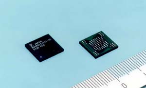
 Tokyo, June 21, 2001---Fujitsu announced today that it has developed the industry's first triple-stacked multi-chip package (MCP), combining 64Mb NOR-type flash memory, 16Mb mobile FCRAM1 with an asynchronous SRAM-type interface, and 4Mb SRAM. The new product (MB84VR5E3J1A1) will go on sale starting today.
Recent advances in mobile-phone technology have expanded cellular-telephone functions to include capabilities such as web browsing and downloading of Java applets2, generating demand for increased memory and higher speeds.
The triple-stacked MCP addresses these new needs by packaging together a flash memory for program and data storage, high data-capacity FCRAM as working memory, and SRAM as cache memory for backup storage when downloading data or when the device is in standby mode. This combination enables efficient memory usage to accommodate greater functionality and data capacity in cellular telephones.
The MCP also achieves a reduction in the amount of power used by the combined memory chips and minimizes the number of parts and amount of wiring required by common data bus widths. The package size (PBGA3 85: 10.4 x 10.8 x 1.3mm) is slightly slimmer than conventional MCPs, and, because it combines three chips into one, it uses a 30% smaller board area than previous models.
| Sample Price | : | 7,000 yen (tax not included) |
| Availability | : | Sample: June 21, 2001
Mass Production: September 2001 |
| Sales Target | : | 500,000 units/month |
Main Features:
- 1. Product Configuration: Number of data buses x 16
- 64Mb NOR-type flash memory/16Mb mobile FCRAM/4Mb SRAM
2. Access Time:
- Address access/program (1 word)
max. 85 nanoseconds/standard 16 microseconds (NOR-type flash memory)
- Random read access
max. 90 nanoseconds (mobile FCRAM)
max. 85 nanoseconds (SRAM)
3. Power Supply: Vcc=2.7V to 3.1V
4. Low Power Consumption
- Standby Mode:
max. 5 microamps (NOR-type flash memory)
max. 70 microamps (mobile FCRAM)
max. 7 microamps (SRAM)
- Power-Saving Mode:
max. 10 microamps (mobile FCRAM)
- Read Operation:
max. 18 milliamps (5 MHz, NOR-type flash memory)
max. 20 milliamps (11MHz, mobile FCRAM)
max. 40 milliamps (10MHz, SRAM)
- Write/Erase Operations:
max. 40 milliamps (NOR-type flash memory)
- Erase/Write Cycles:
100,000 (NOR-type flash memory)
5. Packaging: standard plastic BGA 85 balls
Glossary:
- Mobile FCRAM (Fast-Cycle Random Access Memory): Developed by Fujitsu, FCRAM is a next-generation memory-core technology that incorporates an asynchronous SRAM-type interface and enables reduced power consumption for mobile communications devices.
- Java applet: Java is an object-oriented programming language developed by Sun Microsystems, Inc., in the United States. Java applets are programs operated through Internet browsers and can be downloaded from Internet servers to add animated images and sounds to websites.
- PBGA (Plastic Ball Grid Array): A type of surface-mountable plastic packaging.
Trademarks:
FCRAM is a registered trademark of Fujitsu Ltd.
All other company/product names mentioned are trademarks or registered trademarks of their respective holders.

About Fujitsu
Fujitsu is a leading provider of Internet-focused information technology solutions for the global marketplace. Its pace-setting technologies, best-in-class computing and telecommunications platforms, and worldwide corps of systems and services experts make it uniquely positioned to unleash the infinite possibilities of the Internet to help its customers succeed. Headquartered in Tokyo, Fujitsu Limited (TSE:6702) reported consolidated revenues of 5.48 trillion yen for the fiscal year ended March 31, 2001.
Internet: http://www.fujitsu.com/
|