 Tokyo, June 19, 2000 - Fujitsu unveiled today two 32Mbit dual-
operation flash memory products (MBM29DS323TE and MBM29DS323BE), jointly developed with Advanced Micro Devices (AMD). Running on a 1.8V single power source, the new devices
can simultaneously perform read, write and erase functions. Sample shipment starts today, with volume shipment scheduled to begin in late September.
Tokyo, June 19, 2000 - Fujitsu unveiled today two 32Mbit dual-
operation flash memory products (MBM29DS323TE and MBM29DS323BE), jointly developed with Advanced Micro Devices (AMD). Running on a 1.8V single power source, the new devices
can simultaneously perform read, write and erase functions. Sample shipment starts today, with volume shipment scheduled to begin in late September.
Dual-operation flash memory products, including Fujitsu's 1.8V
single power source 8M/16Mbit models already on the market, have
enjoyed increasing demand for use in cellular phones and mobile
information terminals, which require high-speed processing and
frequent rewriting, and lower-voltage devices are more and more
in demand.
Responding to these needs, Fujitsu's newly developed 32Mbit
dual operation flash memory devices run on a 1.8V single power
source and boast high-speed access time of 100 nanoseconds. In
addition, they offer such features as a Hi-ROM *1 (Hidden Read
Only Memory) function that prevents illegal copying and an
accelerator function that enables faster write time at system
load-in.
A leader in the flash memory market, Fujitsu will continue to
set the pace in developing and commercializing a variety multi-
function, energy-saving flash memory products, and in making
possible further reductions of power consumption for multi-
function mobile devices.
Sample pricing:
- 32Mbit dual operation flash memory: 4,000 yen (TSOP *2)
Sales target (MBM29DS323TE and MBM29DS323BE combined):
- 1 million units per month
Specifications:
- Process technology: 0.23 micron CMOS process
- Cell structure: two-layer polysilicon structure NOR type memory cell
- Output: 2M word x 16 bit/ 4M byte x 8 bit (32Mbit)
- Sector size:
| Bank1 | 8M bit |
| Bank2 | 24M bit |
- Security: Hi-ROM function to prevent illegal copies.
- Hi-ROM area: 64Kbyte
- WP#/ACC functions (WP#: WP upperbar)
WP#: protects part of boot sector on Bank 1 (8Kbytes x 2)
ACC: reduces write time when external high voltage is applied
- Common Flash Memory Interface (CFI)
- Access Time [MBM29DS323TE/BE]
Address access: 100/120 nanosecond (max.)
CE# (CE upperbar) access: 100/120 nanosecond (max.)
OE# (OE upperbar) access: 35/50 nanosecond (max.)
- Single power operation: 1.8V to 2.2V
- Low power consumption
Automatic sleep mode
stand-by mode: 1 micro ampere (standard)
read mode: 16 milli-ampere (max.) word mode f=5MHz
write/erase mode: 25 milli-ampere (max.)
- Number of erase / write operations: 100,000 (min.)
- Boot block sector architecture
MBM29DS323TE: boot block in top address
MBM29DS323BE: boot block in bottom address
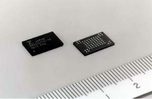
- Packaging: standard 48 pin plastic TSOP package standard
63 ball/ FBGA *3 package
Glossary
| *1 | Hi-ROM (Hidden Read Only Memory): Input area for security codes and particular information |
| *2 | TSOP (Thin Small Outline L-Leaded Package): A thin-surface packaging |
| *3 | FBGA (Fine-pitch Ball Grid Array): A surface-mount packaging with less than 1.0 mm of space between ball terminals. |
About Fujitsu Limited
Fujitsu Limited (TSE: 6702) is a leading provider of Internet-based
information technology solutions for the global marketplace.
Comprising over 500 group companies and affiliates worldwide --
including ICL, Amdahl and DMR Consulting -- it had consolidated
revenues of 5.26 trillion yen (US$49.6 billion) in the fiscal year
ended March 31, 2000. Fujitsu's pace-setting technologies, world-
class computing and telecommunications platforms, and global corps
of over 60,000 systems and services experts make it uniquely
positioned to unleash the infinite possibilities of the Internet to
help its customers succeed. Altogether, the Fujitsu Group has
188,000 employees and operations in over 100 countries.
Internet: http://www.fujitsu.com/
Fujitsu: The Possibilities Are Infinite
* All company/product names mentioned may be trademarks or
registered trademarks of their respective holders and are used
for identification purpose only.