 |
Fujitsu Laboratories Ltd.
Fujitsu Limited
Fujitsu Develops Advanced Printing Bump Technology
Enables Production of Lead-Free Fine Solder Bumps at Half the Cost
|
 Tokyo, December 12, 2001---Fujitsu Laboratories Ltd. and Fujitsu Limited announced today that they have developed an Advanced Printing Bump (AP Bump) technology, which allows for fine-pitch solder bumps to be formed directly on to a semiconductor wafer prior to dicing, at less than half the cost of conventional bump technology.
For compact consumer products like cellular phones, the new technology enables the use of high-performance, high pin-count chips and the creation of extremely small and lightweight products with improved performance. The lead-free solder paste(*1) used for the bumps meets environmental WEEE/ROHS directives. This technology is already available in engineering samples and will go into mass production in January 2002.
Background
The high performance, high pin-count chips used in equipment such as high-end severs and networking have been flip-chip(*2)-mounted with solder bumps covering the entire chip surface, to improve the signal and power/ground integrity. As chips have achieved higher levels of integration in recent years, pin-counts have risen as well, and the spacing between solder bumps has decreased to today's 200 µm. This has created a need for a technology that can form fine-pitch bumps at lower cost.
There are two general approaches to forming solder bumps: vapor deposition and plating. Vapor deposition requires a considerable investment in heavy equipment and has high running costs, making it unsuitable for mounting low-cost packages. Plating has low process costs, but not all solders are compatible with this technique.
More recently, a new approach, known as solder paste printing, has been gaining notice. This is an economical way to produce solder bumps, but the disadvantage is that it has been difficult to form fine-pitch bumps less than 200 µm, and this method also entails limitations on bump height.
With bump pitches expected to be as tight as 120 µm in a few years, there is a clear demand for a technology that is low-cost, lead-free, and supports fine-pitch bumps.
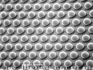
About the New Technology
AP Bump technology uses photo-sensitive film(*3) and solder paste in the bumping process. The advantages of this approach are:
- This technology enables the formation of uniform, fine-pitch bumps, and the technology can already be used for 120 µm-pitch bumps, and developments are expected to push this to 100 µm in 2002.
- This technology also allows the formation of tall bumps, e.g., the formation of 130-µm tall bumps with a 220µm pitch in 2002, which is expected to improve to 150-µm tall bumps.
- Bumps can be formed at a considerable cost savings, because an entire wafer can be bump printed prior to dicing.
- Because solder paste is used, products can easily be made lead-free.
The development of this new process for applying solder bumps to high pin-count chips is a step towards more compact, higher performance electronic equipment with lower cost.
Glossary
- *1 Solder paste:
- A soldering material in paste form that consists of solder powder, rosin, solvent, activator, thickener, and other flux ingredients.
- *2 Flip-chip:
- A mounting technique in which the chip is inverted and then joined to the circuit board. Solder bumps are applied to either the chip or the circuit board at this point, and the chip is joined with the board through these bumps.
- *3 Photo-sensitive film:
- Technically referred to as a photosensitive dry film resist, this uses a photographic exposure or imaging process to create holes in a mask pattern.

About Fujitsu Laboratories Ltd.
Founded in 1968 as a wholly owned subsidiary of Fujitsu Limited, Fujitsu Laboratories Limited is one of the premier research centers in the world. With a global network of laboratories in Japan, China, the United States and Europe, the organization conducts a wide range of basic and applied research in the areas of Multimedia, Personal Systems, Networks, Peripherals, Advanced Materials and Electronic Devices.
About Fujitsu
Fujitsu is a leading provider of Internet-focused information technology solutions for the global marketplace. Its pace-setting technologies, best-in-class computing and telecommunications platforms, and worldwide corps of systems and services experts make it uniquely positioned to unleash the infinite possibilities of the Internet to help its customers succeed. Headquartered in Tokyo, Fujitsu Limited (TSE:6702) reported consolidated revenues of 5.48 trillion yen for the fiscal year ended March 31, 2001.
Internet: http://www.fujitsu.com/
|
Please understand that product prices, specifications and other details are current on the day of issue of the press release, however, may change thereafter without notice.

|