 Tokyo, August 2, 2001 ---Fujitsu Limited today announced that it has succeeded in developing mass-production technology for non-volatile ferroelectric random access memory (FRAM)(*1) using 0.35-micron process technology - an industry first. In addition, using this FRAM process technology, the company has developed and will today begin sales of a new LSI chip (MB94R202) for multi-functional IC cards that integrates a 32bit CPU and 512kbit (64kbyte) FRAM.
In recent years, IC cards have come to be used in a variety of applications, including as ID cards, financial cards, and mass transit and toll collection cards. The overall market for IC cards is projected to expand to about 8 billion cards by the year 2005 as more functions, including e-commerce capability, are added and the cards are more widely circulated. Currently, EEPROM is the primary memory device used to store data in IC cards, but Fujitsu's FRAM is superior to EEPROM in many respects, including a write speed about 10,000 times faster. In addition, FRAM consumes 1/400th of the power EEPROM uses for writing data, and its rewrite endurance is 100,000 times greater. Moreover, the integration of FRAM and a CPU makes it possible to create an extremely secure system, allowing data encryption for e-commerce transactions over the Internet, as well as personal authentication through public keys.
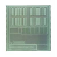
MB94R202 LSI Chip
Fujitsu's newly introduced MB94R202 LSI chip contains a 32-bit RISC processor and can support an OS designed for multi-application management. The incorporation of large-capacity 64kByte FRAM makes it possible to carry out multiple applications and store large amounts of data. Furthermore, the new product is a "combination card," which incorporates both contact and contactless communications interfaces and uses a reader/writer communications protocol that complies with ISO standards. The chip offers a high level of security thanks to the use of elliptic curve cryptography (*2), DES (*3), RSA (*4), and other methods as the encryption circuit technology for carrying out user authentication. Featuring a design that takes maximum advantage of FRAM's special characteristics - including high speed, low power consumption, and superior rewrite ability - the new device enables numerous applications to be executed at high speeds and with very low power consumption, making it ideal for use in multi-functional IC cards in the burgeoning broadband Internet era.
Sample shipments begin today (sample priced at 1,200 yen), with volume production to start from January 2002. Fujitsu has set a sales target of 1.5 million units/month from first half of FY2002.
Principal Specifications:
- 32bit RISK CPU
- 96kBytes mask ROM (program memory)
- 4kBytes SRAM (working memory)
- 64kBytes FRAM (data memory)
- Contact mode: ISO7816, T=0,1
- Contactless mode: ISO14443-TypeB, T=CL
- DES, elliptical curve cryptography (ECC), RSA
- Java OS (set to use)
Fujitsu's 0.35-Micron Ferroelectric Technology
Fujitsu began mass-producing FRAM devices utilizing 0.5-micron technology in October 1999 and has shipped over 30 million FRAM products to date. The company's groundbreaking new 0.35-micron FRAM technology achieves not only greater memory density but also improved write speed, power consumption, and rewrite endurance.
In developing the new technology, Fujitsu focused its efforts on devising methods to improve the process technology by enhancing the performance characteristics of PZT (*5) crystals and electrodes and developing a unique protective film to eliminate the PZT degradation during the manufacturing process. Fujitsu worked together with an equipment manufacturer to develop specialized devices for PZT sputtering and etching - key FRAM fabrication processes. By doing so, Fujitsu was able to begin volume production of 0.5-micron FRAM devices, and, after additional improvements, to achieve stable mass production of 0.35um FRAM. In addition, Fujitsu's 0.5- and 0.35-micron FRAM device process was constructed by simply adding a PZT capacitor fabrication process to the usual CMOS logic process. This method enabled FRAM and CMOS logic to be easily combined at low cost and existing design aspects to be preserved.
Glossary:
- *1 FRAM (Ferroelectric Random Access Memory):
- A non-volatile memory device using ferroelectric materials that is able to retain data even when the power is turned off. Can write at high speeds and rewrite numerous times with very low power consumption.
- *2 Elliptic Curve Cryptography:
- A public key encryption method developed by Koblitz and Miller.
- *3 DES (Data Encryption Standard):
- A common data encryption method.
- *4 RSA (Rivest Shamir Adleman):
- A public key encryption method devised by Rivest, Shamir, and Adleman.
- *5 PZT (PbZrTiO):
- A ferroelectric substance (lead zirconate titanate)
Note: FRAM is a registered trademark of Ramtron International Corporation. Java is a registered trademark of Sun Microsystems, Inc. All other company/product names mentioned may be trademarks or registered trademarks of their respective holders

About Fujitsu
Fujitsu is a leading provider of Internet-focused information technology solutions for the global marketplace. Its pace-setting technologies, best-in-class computing and telecommunications platforms, and worldwide corps of systems and services experts make it uniquely positioned to unleash the infinite possibilities of the Internet to help its customers succeed. Headquartered in Tokyo, Fujitsu Limited (TSE:6702) reported consolidated revenues of 5.48 trillion yen for the fiscal year ended March 31, 2001.
Internet: http://www.fujitsu.com/
|