Fujitsu Labs Develops New DRAM Cell Structure
--Reversed-Stacked-Capacitor Cell
Suitable for the Gigabit-Era System-on-a-Chip
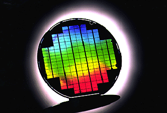

In the new cell structure, as with conventional stacked cells, the capacitor is fabricated on top of a MOS transistor and the surface of the wafer is bonded to a separate support substrate. Then, CMP (Chemical Mechanical Polishing) technology is used to remove the silicon layer of the wafer surface directly below the MOS transistor, where a new flat surface is delineated. And since the metal wiring is formed on this new surface, loading of the DRAM together with the MPU on the same chip is made significantly easier.
With this structure, researchers were able to successfully fabricate a test memory cell device using a 0.35 micron design rule for a 64Mb DRAM and to confirm the structure's capability to achieve higher speeds and lower power consumption. The new structure is called a Reversed-Stacked-Capacitor Cell, because the positioning of the capacitor and MOS transistor are inverted.
In addition, researchers believe that this reversed structure MOS transistor can be used to achieve a low power logic LSI for the multimedia age, and that it can be converted to a SOI-type (Silicon-On-Insulator) MOS transistor.
The three principle advantages of the new structure are as follows:
These advantages make possible the previously difficult feat of combining MPU and DRAM, thus marking, an important step forward toward achieving a system on a chip.
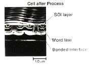
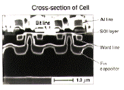
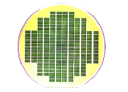
To realize the new structure, a new CMP (Chemical Mechanical Polishing) technology was developed, which enabled a 0.6 mm-thick silicon wafer to be trimmed to the thickness of a MOS transistor--100 nm.
Fujitsu Laboratories Ltd. will present a paper on the Reversed-Stacked-Capacitor Cell structure on December 12 at the International Electron Devices Meeting '95 (IEDM'95) in Washington D.C.
The company is applying for 13 patents related to the newly developed technology.
Isao Hirano, Mike Beirne
Fujitsu Limited, Public Relations
6-1 Marunouchi 1-chome, Chiyoda-ku
Tokyo 100 Japan
Tel: +81-3-3213-4160
Fax: +81-3-3216-9365
Internet e-mail: hirano@hq.fujitsu.co.jp, mike@hq.fujitsu.co.jp
Internet server: http://www.fujitsu.com/