 |
| [ PRESS RELEASE ] |
2003-0013E
Fujitsu Limited
|
Fujitsu Unveils 40Gbps LN Optical Modulator with 1.8V Drive Voltage
Key component for low cost optical transmission boasts
world's lowest drive voltage
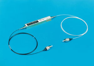
 Tokyo, January 21, 2003 - Fujitsu Limited today announced the introduction of a new 40Gbps LN optical modulator (*1) with 1.8V drive voltage - lowest of its kind in the world.
The newly developed modulator, one of the key components in an optical transmitter, converts the electrical data signal to an optical data stream. The introduction of this product enables optical transmitters to meet the low cost, small-form-factor and low power requirements of next-generation 40Gbps optical communications systems.
The product comes in two models: The 40Gbps Dual-Drive LN Optical Modulator (*2) and the 40Gbps Single-Drive LN Optical Modulator (*2). Samples for system evaluation go on sale today, with actual shipments expected to begin in April. Volume shipments are slated for August 2003.
Special Features of Fujitsu's New Modulator
- Ultra low drive voltage: 1.8V for dual-drive model; 3.5V for single-drive model
The 3.0V drive voltage of conventional dual drive optical modulators (5.5V in the single-drive models) requires that custom drive amplifiers with high output voltages and wide bandwidths be used to operate them. This product, which has achieved a drastic reduction in drive voltage, removes this requirement. Standard drive amplifiers can now be used in 40Gbps optical transmission systems. This modulator will enable low cost, small-form-factor, low power consumption 40Gbps optical transmitters to now be developed.
- Built-in PD (photodiode) for monitoring the optical output signal
In LN modulators, monitoring of the optical output signal is necessary to adjust the modulator control DC bias (*3). The built-in monitor PD eliminates the need for the external optical monitoring circuit that is required for most modulators.
- Separate DC bias terminal
This new modulator has separate input terminals for the electrical data and DC bias control. This design removes the requirement for the external circuitry that combines the data signal and the DC bias.
Fujitsu's new LN modulator will be on display at the 3rd Fiber Optics EXPO, January 22 to 24 in Japan. http://www.reedexpo.co.jp/foe/english/
Sales outside Japan are handled through Fujitsu Quantum Devices Limited and its sales subsidiaries Fujitsu Compound Semiconductor, Inc., Fujitsu Quantum Devices Europe Ltd., and Fujitsu Quantum Devices Singapore Pte. Ltd.
Glossary
- *1. LN optical modulator
-
A device that converts an electrical data signal into an optical data stream via the electro-optic effect of a LiNbO3 crystal. Input electrical "0", "1" signals are converted to the optical signals "ON", "OFF". One of the LN modulator's features is modulation with minimal wavelength chirping. This is a desirable characteristic for ultra high-speed, long haul, and WDM (Wavelength Division Multiplexing) transmission. For this reason, LN modulators are widely adopted in next-generation 40Gbps transmission systems, terrestrial trunk transmission systems, and submarine transmission systems.
- *2. 40Gbps Dual-Drive LN Optical Modulator, 40Gbps Single-Drive LN Optical Modulator
-
Dual-drive devices are driven by 2 electrical complementary signals (for example, "1001" and "0110"). Single-drive devices work with a single electrical signal being input.
Both types of LN modulators are available from Fujitsu to meet customer's requirements.
- 3. Modulator control DC bias
-
To achieve optimum operation from a LN modulator, a DC voltage (modulator control DC bias) must be applied in addition to the data signal. Since the optimum DC bias drifts over time, the modulator control DC bias must be adjusted by monitoring the optical output signal from the modulator.
About Fujitsu
Fujitsu is a leading provider of customer-focused IT and communications solutions for the global marketplace. Pace-setting technologies, high-reliability/performance computing and telecommunications platforms, and a worldwide corps of systems and services experts make Fujitsu uniquely positioned to unleash the infinite possibilities of the broadband Internet to help its customers succeed. Headquartered in Tokyo, Fujitsu Limited (TSE:6702) reported consolidated revenues of 5 trillion yen (about US$38 billion) for the fiscal year ended March 31, 2002. For more information, please see: http://www.fujitsu.com/
[Press Contacts]
- Fujitsu Limited
-
Public & Investor Relations
Kouyou Nishi, Nancy Ikehara
Tel: +81-3-3215-5259 (Tokyo)
 Press Inquiries Press Inquiries
|
[Technical contacts:]
- Fujitsu Limited
-
Peripheral Products Sales Dept.
Peripheral Products Business Division
Platform Business Development and Management Group
1-1, Kamikodanaka 4-chome, Nakahara-ku, Kawasaki
211-8588, Japan
TEL: +81-44-754-8347
E-MAIL: j.hasegawa@jp.fujitsu.com
- Fujitsu Quantum Devices Ltd.
-
Overseas Direct Sales Department
11th Floor, Hachioji Daiichi-Seimei Bldg.
3-20-6 Myojin-cho
Hachioji-city, Tokyo 192-0046, Japan
TEL: +81-426-43-5885
E-MAIL: www-sales@fqd.fujitsu.com
- Fujitsu Compound Semiconductor, Inc.
-
2355 Zanker Road, San Jose, CA 95131-1138, U.S.A.
TEL: +1-408-232-9500
E-MAIL: sales@fcsi.fujitsu.com
- Fujitsu Quantum Devices Europe Ltd.
-
Network House, Norreys Drive.
Maidenhead, Berkshire, SL6 4FJ, UK
TEL: +44-1628-504-800
E-Mail: LWSales@fqde.fujitsu.com
- Fujitsu Quantum Devices Singapore Pte. Ltd.
-
Hong Kong Branch
Rm. 1101, Ocean Centre, 5 Canton Road,
Tsim Sha Tsui, Kowloon, Hong Kong.
TEL: +852-2377-0227
E-MAIL: hksales@fqdshk.com.hk
|
All company/product names mentioned may be trademarks or registered trademarks of their respective holders and are used for identification purpose only.
Please understand that product prices, specifications and other details are current on the day of issue of the press release, however, may change thereafter without notice.

|
 |

