|
|
Fujitsu Limited |
|
Fujitsu Designs World's Smallest Chip-Size Module Adopting Advanced System-in-Package Technology
 Tokyo, June 6, 2002 - Fujitsu Limited today announced that it has developed an LSI package CS Module(TM), or chip-size module, incorporating cutting-edge system-in-package (SiP) technology capable of shrinking the size of a multi-chip package to that of the largest chip contained in it. The company is the first in the world to successfully develop a prototype package.
The new module combines advances in wafer thinning technology, which reduces the thickness of existing chips by about 16%, with chip stacking and re-distribution technologies. Compared to SiPs with similar functionalities, the prototype chip boasts a 30% reduced board area and 65% thinner profile, making it the ideal system LSI solution for miniaturized digital equipment.
Background
As mobile phones, PDAs, and digital A/V equipment continue to shrink in size while growing in functionality, there is ever-increasing demand for system LSI solutions that offer short development cycles. System LSI design uses the system-on-chip (SoC) approach, which integrates multiple functions into a single chip, and system-in-package (SiP) approach, in which several independent ICs are stacked on to the substrate. SiPs, by utilizing existing assembly infrastructure, offer the advantage of delivering low cost LSI products in a short period of time. However, the need for interposers*1, such as tape substrate*2, and wire bonding for fine pitch interconnections, poses limitations to compact system design.
About the New Technology
Fujitsu's new packaging technology drastically reduces the size of conventional SiPs by fabricating thin-profile chips and, after stacking them into two layers, re-distributing signal circuitry between the chips. Leveraging these core technologies enabled the company to successfully design a system LSI prototype that combines logic and memory functions, for high-end applications.
Figure 1 shows a CS Module for high-end applications. This places a second logic device on top of the first, plus a memory device (the prototype includes four chips). The upper-stage chip spacing is at a 0.040 mm pitch. Employing 0.050 mm thick chips, the module achieves a maximum density of only 0.65 mm.
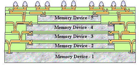
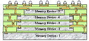
Figure 2 shows a schematic of 5-layer high capacity memory product with four chips stacked on top of the base-level memory device.
Special Features of New Technology
The new technology is a combination of several technologies:
- Wafer level chip size package (CSP) processing technology - CSP is the package whose size is equal to or slightly larger than the chips housed in it. Wafer-level CSP is the package whose entire assembly process is completed at the wafer level. Comprises of a wiring formation technology for signal transmission, device-protecting passivation technology*3, and the external terminal formation technology needed to attach the device to the motherboard.
- Ultra-thin wafer processing technology - enables ultra thin wafer densities by mechanically grinding the rear face of the wafer from the standard thickness of 0.15 mm to 0.025 mm, a reduction by approximately 16%.
- High precision placement technology - permits mounting of ultra-thin chips on wafer at a tolerance of ±0.005 millimeters, with the aid of a chip bonder.
- Interchip planarization technology - allows re-distribution between multi-level chips by padding embedding resin in gaps between chips placed on a wafer surface for greater planarity.
- Re-distribution technology -forms fine copper circuits by exposing, developing and etching processes.
- Built-in passive components technology - enables inclusion of capacitor and inductor by using re-distribution technology.
Figure 1: Chip-size module structure, high-end application

Figure 2: Chip-size module structure, memory-stack application
[Click to enlarge]
Glossary
- 1. Tape substrate
- A substrate made by forming a thin layer of copper traces on a thin-film polyimide tape. Has the advantage of flexibility, and is widely used, not only for packaging, but also for printer drivers and other circuit-board applications.
- 2. Interposer
- A thin subtrate used in chip-size packages, generally made of polyimide tape or glass epoxy thin core.
- 3. Passivation technology
- Top cover protection film that relaxes mechanical stress to LSI chip surface and prevents short circuits during solder mounting.
* CS Module is a trademark of Fujitsu Limited. All other product names and company names mentioned herein are the trademarks or registered trademarks of their respective firms.
About Fujitsu
Fujitsu is a leading provider of customer-focused IT and communications solutions for the global marketplace. Pace- setting technologies, high-reliability/performance computing and telecommunications platforms, and a worldwide corps of systems and services experts make Fujitsu uniquely positioned to unleash the infinite possibilities of the broadband Internet to help its customers succeed. Headquartered in Tokyo, Fujitsu Limited (TSE:6702) reported consolidated revenues of 5 trillion yen (about US$38 billion) for the fiscal year ended March 31, 2002. For more information, please see: http://www.fujitsu.com/
 |
 |
[Press Contacts]
Minoru Sekiguchi, Nancy Ikehara
Fujitsu Limited, Public & Investor Relations
Tel: +81-3-3215-5259 (Tokyo)
Fax: +81-3-3216-9365
 Press Inquiries Press Inquiries
|
[Customer Contact]
Fujitsu Limited, Electronic Devices Group
LSI Packaging Division
Advanced Packageing Technology R&D Department I
Tel: +81-594-24-5528 (Mie)
E-mail: edevice@fujitsu.com
|
|
|
|
| Please
understand that product prices, specifications and other details are
current on the day of issue of the press release, however, may change
thereafter without notice. |
|