| [ PRESS RELEASE ] |
Fujitsu Laboratories Ltd.
Fujitsu Limited
|
Fujitsu Develops World's First CMOS Interface Technology for
10Gbps Parallel Transmissions
Tokyo, February 25, 2003 -- Fujitsu Laboratories and Fujitsu Limited today announced the development of the world's first CMOS parallel-interface device for use in standard logic LSI devices to enable high-speed, multi-channel transmissions at speeds of up to 10Gbps.
Use of the new technology will enable servers, storage devices and communications equipment to handle even larger amounts of data at higher speeds while consuming less power. It is expected to lead to a dramatic increase in the speed and performance of network systems.
Details on this technology were presented at ISSCC 2003 (International Solid-State Circuits Conference), which opened February 10 in San Francisco.
Background
With the spread of broadband Internet access, it is not just communication networks that need to be upgraded to handle increasing data volumes at higher speeds. Technology for transmitting high-volume, high-speed data signals within communications equipment, servers and storage devices has also become increasingly important. Today's leading-edge equipment can handle up to 2.5Gbps per channel, but within the next few years processing speeds are expected to increase to 6.4Gbps, or even 10Gbps.
In the past, transmissions in the gigabit range required specialized high-speed devices, such as silicon germanium and other compound semiconductors, but their high cost and energy demands had been deemed problematic. CMOS-based high-speed interfaces offer an ideal solution, not only because of their lower energy requirements, but also because these interfaces can be readily integrated with system-on-chip devices and ASICs, reducing overall system energy demands and costs further still.
Fujitsu had previously succeeded in developing a 3.125Gbps interface circuit using a 0.11 µm CMOS process. The next step was to develop circuit technology capable of handling speeds of 6.4Gbps or 10Gbps using the same process technology.
About the Technology
Optimized for the 0.11 µm CMOS process, Fujitsu's low-voltage CMOS interface technology enables high-speed operation and low power consumption without requiring any additional special steps in the fabrication process. In addition, the development of the world's first circuit architecture that is highly expandable to accommodate multiple channels makes it possible to transmit large capacities of data via parallel interface.
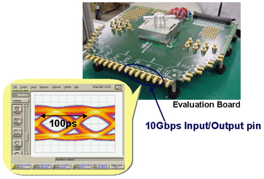
The fabricated interface circuit was tested with four 10-Gbps input channels and output channels each clustered together, and found to require only 1240 mW of power, or 310 mW per channel. In addition, it has a clock-regeneration circuit embedded to enable multi-channel transmissions, and tests confirmed that it meets the SONET OC-192(*1) performance standards for jitter-tolerance(*2).
Fujitsu's new technology has the following distinctive features:
- High speed operation at low power with one 1.2-V source.
- High degree of chip integration, with 10 million+ gates using standard 0.11 µm CMOS process technology.
- Readily expandable architecture to handle multiple channels.
This technology makes it possible to add high-speed signal transfer channels to standard, highly integrated logic chips, making them ideal for use in high-performance communications equipment, servers and storage devices at a very low cost. Commercial products incorporating the technology are expected to be introduced later this year.
 Glossary
- *1. SONET OC-192
- SONET is the name for the North American optical communication standards. OC-192 is the specification for 10Gbps transport.
- *2. Jitter tolerance
- Temperature, circuitry variations, and other factors can cause frequency discrepancies between the clock used at the receiving interface and the clock used at the data-transmitting end. Jitter tolerance is the range of variation that can be tolerated.
About Fujitsu Laboratories Ltd.
Founded in 1968 as a wholly owned subsidiary of Fujitsu Limited, Fujitsu Laboratories Limited is one of the premier research centers in the world. With a global network of laboratories in Japan, China, the United States and Europe, the organization conducts a wide range of basic and applied research in the areas of IT Core Systems, IT Media, Networks, Peripherals, Advanced Materials and Electronic Devices.
About Fujitsu
Fujitsu is a leading provider of customer-focused IT and communications solutions for the global marketplace. Pace-setting technologies, high-reliability/performance computing and telecommunications platforms, and a worldwide corps of systems and services experts make Fujitsu uniquely positioned to unleash the infinite possibilities of the broadband Internet to help its customers succeed. Headquartered in Tokyo, Fujitsu Limited (TSE:6702) reported consolidated revenues of 5 trillion yen (about US$38 billion) for the fiscal year ended March 31, 2002. For more information, please see: http://www.fujitsu.com/
[Press Contacts]
Minoru Sekiguchi, Nancy Ikehara
Fujitsu Limited, Public & Investor Relations
Tel: +81-3-3215-5259 (Tokyo)
Fax: +81-3-3216-9365
 Press Inquiries Press Inquiries
|
[Technical Contact]
Fujitsu Laboratories Ltd.
Kohtaroh Gotoh
System LSI Development Laboratories
Tel: +81-44-754-2723
E-mail: kohta@jp.fujitsu.com
|
All company/product names mentioned may be trademarks or registered trademarks of their respective holders and are used for identification purpose only.
Please understand that product prices, specifications and other details are current on the day of issue of the press release, however, may change thereafter without notice.

|
