| [ PRESS RELEASE ] |
2002-0273E
Fujitsu Laboratories Ltd.
ujitsu Component Ltd.
|
Fujitsu Develops Touch Panel Screen with Light Transparency of 98%
Using Surface Acoustic Waves
 Tokyo, November 26, 2002- Fujitsu Laboratories Ltd. and Fujitsu Component Ltd. announced today that they have succeeded in using surface acoustic waves(*1) (SAWs) generated by a piezoelectric thin-film transducer(*2) to develop a touch panel screen ideally suited for use in mobile information and communication devices such as PDAs, a world's first.
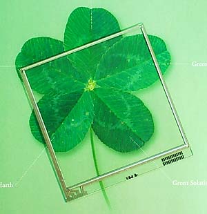
The newly developed touch panel has a thickness of 0.7mm and uses a single glass substrate having a 1.4mm-wide frame, where the piezoelectric thin-film transducer is housed. Achieving a light transparency ratio of 98%, it enables excellent visibility, is scratch resistant, and can be made very compact.
Details of this technology will be announced at the meeting of the Ultrasonic Technical Group of the Institute of Electronics, Information and Communication Engineers to be held on November 29th at Shizuoka University.
Background
As mobile information and communication devices such as PDAs have adopted color displays and technically advanced functions, demand has increased for displays that can reproduce images with more natural colors. In order to avoid degradation of the display quality in devices that use touch panels, light transparency of the panel must be as high as possible and light reflectance minimal.
In the widely used resistive film method, a touch panel is formed from multiple layers, and light becomes scattered as it passes through each layer. Consequently the light transparency ratio is usually around 82%. Moreover, even with coating treatment on each layer, this ratio has only been able to be improved to approximately 86%.
Although it has been recognized that the SAW method could be applied to achieve a touch panel with a single transparent substrate, until now this has required a wide frame to allow for scanning of the entire substrate surface and the housing of piezoelectric transducers that generate the acoustic waves, thus making it difficult to implement in a small-size panel for mobile device use.
About the Technology
To overcome these hurdles, Fujitsu has newly developed an electrode structure that enables highly accurate detection of the touched position even for narrow panel frame widths, a position detection circuit, and process technology for fabricating the piezoelectric thin-film transducers that convert electrical signals into SAWs.
Because the newly developed touch panel is constructed with a single glass substrate, it achieves 98% light transparency (a 16% improvement over prior touch panels) while maintaining compact dimensions, with a frame width of 1.4mm (approximately half the prior width) and a thickness of 0.7mm.
Special features of the newly developed technology are listed below.
- The world's first transducer structure that enables highly accurate position detection within a narrow frame
Utilizing a single-phase transducer(*3) (SPT) electrode structure in which a piezoelectric thin-film is sandwiched between an electrode and a unipolar comb-type electrode, a chevron-shaped electrode structure was devised, consisting of an array of consecutive V-shaped comb-type electrodes. This new structure enabled the realization of a frame width of 1.4mm and highly accurate position detection performance.
- Control circuitry that realizes high resolution
Specialized control circuitry was developed for the piezoelectric thin-film transducer configured from the SPT electrode and chevron-shaped electrode structures. This new control circuitry achieves position resolution of 100 dpi (dots per inch), suitable for hand written input, and a sampling rate of 100 times per second.
- Fabrication process for piezoelectric thin film
A film deposition process was developed to fabricate a piezoelectric thin film suitable for the piezoelectric thin film transducer configured from the abovementioned SPT electrode and chevron electrode. This piezoelectric thin film has a thickness of approximately 2 microns and efficiently converts electric oscillations to mechanical vibrations.
Glossary
- *1 SAW(Surface Acoustic Wave)
-
The wave generated at the surface of an elastic body. SAWs are used in such commercial applications as high-frequency filters for mobile phones.
- *2 Piezoelectric Thin Film Transducer
-
The piezoelectric effect is the phenomenon whereby the application of stress to a specific object causes electric polarization, and conversely, the application of an electric field causes strain or stress to be generated. A piezoelectric thin film transducer is a device that uses this phenomenon to convert electric signals to SAWs and SAWs to electrical signals.
- *3 SPT(Single Phase Transducer)
-
A transducer configured from a piezoelectric film sandwiched between a short-circuit electrode and a comb-type electrode. Only one electrical interconnect is required per surface.
About Fujitsu
Fujitsu is a leading provider of customer-focused IT and communications solutions for the global marketplace. Pace-setting technologies, high-reliability/performance computing and telecommunications platforms, and a worldwide corps of systems and services experts make Fujitsu uniquely positioned to unleash the infinite possibilities of the broadband Internet to help its customers succeed. Headquartered in Tokyo, Fujitsu Limited (TSE:6702) reported consolidated revenues of 5 trillion yen (about US$38 billion) for the fiscal year ended March 31, 2002. For more information, please see: http://www.fujitsu.com/
[Press Contacts]
Minoru Sekiguchi, Scott Ikeda
Fujitsu Limited, Public & Investor Relations
Tel: +81-3-3215-5259 (Tokyo)
Fax: +81-3-3216-9365
 Press Inquiries Press Inquiries
|
[Technical Contact]
Fujitsu Laboratories Ltd.
Peripheral System Laboratories, Media Device Research Group
Tel: +81-78-934-8252
e-mail: nakazawa.fumihi@jp.fujitsu.com
|
All company/product names mentioned may be trademarks or registered trademarks of their respective holders and are used for identification purpose only.
Please understand that product prices, specifications and other details are current on the day of issue of the press release, however, may change thereafter without notice.

|
