|
|
Fujitsu Laboratories Ltd. |
|
Fujitsu Is First to Achieve Vertical Growth and Diameter Control of Multi-layer Carbon Nanotubes on Silicide for MOSFET Electrodes
Tokyo, July 8, 2002-Fujitsu Laboratories Ltd. announced today that it has succeeded in developing technologies for vertical growth and diameter control of multi-wall carbon nanotubes*1 on a silicide layer for constructing MOSFET electrodes (gate, drain, and source). The pathbreaking development is expected to contribute to lower electrical resistance and finer interconnections for next-generation LSIs.
Details are being presented at the International Conference on the Science and Application of Nanotubes (NT'O2), currently being held in Boston, Massachusetts.
Background
Carbon nanotubes are a new atomic-scale type of material with a number of desirable properties that make them especially promising for use in electronics. Focusing on the special electrical advantages of carbon nanotubes, Fujitsu researchers have been investigating how metallic carbon nanotubes can be applied in ultrafine circuit integration.
Carbon nanotubes are usually produced using laser vaporization and arc discharge. However, these techniques do not offer good control over the location and orientation of the nanotubes, or the diameter of the nanotubes themselves.
Technology Highlights
Fujitsu adopts a fabrication technique called plasma enhanced chemical vapor deposition*2, which uses a methane-hydrogen composite gas. Applying an electrical field perpendicular to the substrate during nanotube growth induces the nanotubes to align with the field. Of particular note, the technology for growing vertically aligned tubes directly on the silicide layer-which can be used as MOSFET electrodes-together with varying the composition of nickel (Ni) or cobalt (Co) in the silicide provides a means for controlling the diameter of the tubes. (Fig. 1)
Major technology advantages include:
1. Vertical growth of multi-layer carbon nanotubes
Applying a calibrated electrical field during material growth makes it possible to directly control the orientation of multi-walled nanotubes on either a Ni or Co monosilicide layer*3.
2. Control of multilayer nanotube diameter
By growing nanotubes on a layer of Ni or Co silicide, the diameter of the resultant tubes can be made smaller. Using a monosilicide layer, they can be reduced by about half that of using a thin film of Ni or Co.
3. Nanotubes vertically embedded in pores
Exposing the catalyst (Ni or Co) needed for growing carbon nanotubes in holes (called vias) that act as a connector allows for a bundle of carbon nanotubes to be grown vertically embedded in the holes.
The newly developed technologies are highly compatible with existing semiconductor fabrication processes, suggesting potential for widespread use in electronics. Using nanotubes in vias, for example, could take advantage of the ballistic transport*4 of carriers in nanotubes, which avoids impurity scattering to reduce wiring resistance. It could also avoid the problem of wiring breaks caused by electro-migration*5 that can arise with copper wiring.
Fujitsu intends to further improve the precision and low resistance qualities of its nanotube growth control technologies, working toward the development of technologies for realizing practical devices in a range of electronics applications.
Figure 1: Multi-layer carbon nanotubes grown vertically on a silicide layer
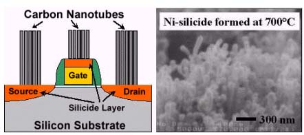
Figure 2: Growing vertically aligned multi-wall carbon nanotubes embedded in a hole

Glossary
1. Multi-wall carbon nanotube
A carbon nanotube is an arrangement of carbon atoms in a two-dimensional hexagonal network (graphene), wrapped into a cylinder, resulting in a tube with a nanometer-scale radius. A multi-wall carbon nanotube comprises several such tubes sharing the same axis. These are expected to have excellent properties, including high aspect ratio, tough mechanical strength, chemical stability, ballistic transport, and a current density permitting electro-migration hundreds of times greater than copper.
2. Plasma enhanced chemical vapor deposition
A technique using gaseous raw materials and a plasma discharge to generate a chemical reaction, depositing the product on a substrate. Excellent ability to generate a thin film on the substrate.
3. Monosilicide layer
Layers formed of a combination of silicon and metal are called "silicides"; when the ratio of metal and silicon is 1:1, it is called a "monosilicide"
4. Ballistic transport
Conduction that is not influenced by impurities or lattice vibration in the conductive carrier. When used in a field-effect transistor, for example, an extremely high-speed and high-frequency operation can be expected.
5. Electro-migration
A phenomenon of metallic materials, whereby matter migrates when electrical currents pass through them. The outbreak of voids and cracks can result in breaks in metallic materials, one of the most serious issues of conduction problems in wiring.
About Fujitsu Laboratories
Founded in 1968 as a wholly owned subsidiary of Fujitsu Limited, Fujitsu Laboratories Limited is one of the premier research centers in the world. With a global network of laboratories in Japan, China, the United States and Europe, the organization conducts a wide range of basic and applied research in the areas of IT Core Systems, IT Media, Networks, Peripherals, Advanced Materials and Electronic Devices.
 |
 |
[Press Contacts]
Minoru Sekiguchi, Robert Pomeroy
Fujitsu Limited, Public & Investor Relations
Tel: +81-3-3215-5259 (Tokyo)
Fax: +81-3-3216-9365
 Press Inquiries Press Inquiries
|
[Technical Contact]
Fujitsu Laboratories Ltd.
Nanotechnology Research Center
Tel: +81-46-250-8234 (Atsugi)
E-mail: y.awano@jp.fujitsu.com
|
|
|
|
All product names and company names mentioned herein are the trademarks or registered trademarks of their respective firms.
Please
understand that product prices, specifications and other details are
current on the day of issue of the press release, however, may change
thereafter without notice. |
|