|
|
Fujitsu Laboratories Ltd. |
|
Fujitsu Develops Non-Volatile FRAM-Based Dynamically Programmable Gate Array
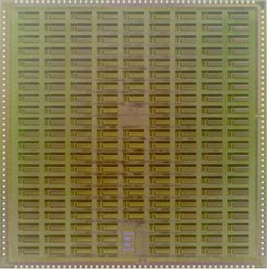 Kawasaki, June 12, 2002-Fujitsu Laboratories Ltd. today announced that it has developed the world's first non-volatile Dynamically Programmable Gate Array (DPGA*1) using ferroelectric RAM (FRAM) technology. This new DPGA has an instant power-on feature made possible by built-in ferroelectric non-volatile configuration memory, and provides a low-cost solution for field programmable devices. In addition, the contents of the configuration memory are kept securely protected to prevent interception or interference. Kawasaki, June 12, 2002-Fujitsu Laboratories Ltd. today announced that it has developed the world's first non-volatile Dynamically Programmable Gate Array (DPGA*1) using ferroelectric RAM (FRAM) technology. This new DPGA has an instant power-on feature made possible by built-in ferroelectric non-volatile configuration memory, and provides a low-cost solution for field programmable devices. In addition, the contents of the configuration memory are kept securely protected to prevent interception or interference.
FPGAs*2 have been attracting significant attention because they enable faster development times and lower development costs compared with mask programmable gate arrays. Since high-end FPGAs use Static RAM (SRAM) technology, their configuration information*3 is lost when the power is shut off. Therefore, conventional FPGAs require off-chip non-volatile PROM or EEPROM to store configuration information. This additional PROM or EEPROM increases the total costs and board area required. Consequently, FPGA users have been eagerly awaiting the development of non-volatile memory technology that supports compatible standard SRAM characteristics.
FRAM technology provides non-volatile devices with perfect matching characteristics for standard CMOS devices. Potential market applications include the chips used for smart cards and as an alternative to battery back-up SRAM. One problem in applying conventional one-transistor/one-capacitor ferroelectric memory to DPGAs, however, is that the access time required is longer than 100 nanoseconds, as a result of the delay associated with the plate line*4. Limited endurance has been another issue, with the number of read cycles limited to 1010 times.
Special Features of the Newly Developed DPGA
- (1) Fast And Non-degradable Read Cycle
- The access time of the configuration memory is comparable to conventional SRAM, and its read operation is non-degradable. This is the first time FRAM-based logic devices have achieved a non-degradable read operation.
- (2) Secure Configuration Protection
- To protect configuration information from interception and overwriting interference, the configuration sequence requires user and message authentication.
- (3) Eight-Way Configuration Memory with Background Programming
- The logic function is configurable eight ways, and the content of the configuration memory can be changed in one-clock cycle without interfering with the logic operation.
With the combination of these technologies, Fujitsu Laboratories has succeeded in developing a high-performance, non-volatile FPGA that is expected to expand the market for FPGAs. In addition, the configuration protection feature makes it possible to ship configured FPGAs without endangering security.
Terminology
- *1 DPGA (Dynamically Programmable Gate Array)
- Can dynamically change its logic operation according to the overall system operation. It has multiple banks of configuration memory corresponding to each function. The available number of logic gates per unit area of DPGA is superior to a conventional FPGA.
- *2 FPGA (Field Programmable Gate Array)
- Gate arrays whose logic function can be configured by users after they have been fabricated. Since FPGAs can immediately run logic circuits right after the synthesizable RTL descriptions have been developed, development times and costs are reduced.
- *3 Configuration Information
- Specifies the logic operation of the FPGA and is stored in the configuration memory.
- *4 Plate Line
- A control line placed on the other side of a storage node of FRAM and used for write and read operations.
About Fujitsu Laboratories Ltd.
Founded in 1968 as a wholly owned subsidiary of Fujitsu Limited, Fujitsu Laboratories Limited is one of the premier research centers in the world. With a global network of laboratories in Japan, China, the United States and Europe, the organization conducts a wide range of basic and applied research in the areas of Multimedia, Personal Systems, Networks, Peripherals, Advanced Materials and Electronic Devices.
 |
 |
[Press Contacts]
Minoru Sekiguchi, Nancy Ikehara
Fujitsu Limited
Public & Investor Relations
Tel: +81-3-3215-5259 (Tokyo)
Fax: +81-3-3216-9365
 Press Inquiries Press Inquiries
|
[Technical Contact]
Fujitsu Laboratories, Ltd.
Silicon Technology Laboratories
Memory Device Laboratory
Tel: +81-42-532-1422 (Tokyo)
E-mail: masui.shoichi@jp.fujitsu.com
|
|
|
|
| Please
understand that product prices, specifications and other details are
current on the day of issue of the press release, however, may change
thereafter without notice. |
|