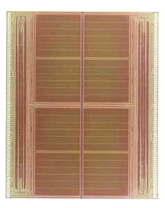
 Tokyo, July 4, 2001 - Fujitsu Limited and Fujitsu VLSI Ltd. announced today that they have jointly developed the industry's first 64-megabit FCRAM with an SDRAM interface for System-in-Package (SiP)*1 applications. The new FCRAM product (MB811L646449) goes on sale starting today.
The new product has a 64-bit bus width, making it ideal for digital appliances requiring large-capacity image processing, such as digital video cameras and DVD recorders. Moreover, optimizing the I/O circuit and memory-cell peripheral circuit for SiP applications has made it possible to achieve a low power supply voltage of 2.5V and a 30% reduction in the operating current (240mA) using identical bandwidth conversions.
In recent years, due to the growth of the digital network-based information society, information systems have increased in functionality, which has led to greater demand for smaller, low-power consuming, and high-performance components within these systems. In response to these demands, there has been a growing focus on SiPs, which combine all types of LSIs, including CPUs, logic, peripheral circuits, and memory, into one package.
Fujitsu's new FCRAM product offers a large bandwidth of 648 Mbyte/second with a clock frequency of 81 MHz x 8 bytes, the standard used by today's image-processing equipment. In addition, the integration of Fujitsu's unique original testing/burn-in simplifier circuit*2 has made it possible to eliminate post-assembly memory tests and early product failures.
The product can be purchased as either a bare chip or a logic LSI-integrated SiP.
-
| Date of Shipment | : | July 4, 2001 (samples only) |
| Sample Price | : | 2,500 yen in Japan (excluding tax) |
| Sales Target | : | 500,000 units/month |
Specifications
-
| Process: | 0.2-micron process, with 3 polysilicon layers and 3 metal layers |
| Power Voltage: | 2.5V  0.2V 0.2V |
| Operating Clock Frequency: |
|
| 81MHz; MB811L646449-12 |
 |
RAS cycle time: | 72ns |
 |
clock access time: | 9ns |
| 54MHz; MB811L646449-18 |
 |
RAS cycle time: | 108ns |
 |
clock access time: | 9ns |
|
| Active Current: | 240mA |
| Bus Width: | x64 bit I/O structure (1Mbit x 32 bit I/O, 2-part structure) |
| CAS Latency: | 2 |
| I/O Interface: | LVTTL*3 |
Terminology
- *1 SiP (System in Package):
- A method of building systems by packaging together multiple LSIs.
- *2 Testing/Burn-In Simplifier Circuit
- A circuit that performs diagnostic tests on chips; circuit that facilitates burn-in tests on wafers.
- *3 LVTTL: Low-Voltage Transistor-Transistor Logic
- Common I/O interface standard for low voltage LSIs.
(VIH [min.] = 2.0V, VIL [max.] = 0.4V)
Trademarks:
FCRAM is a registered trademark of Fujitsu Limited.
All other company/product names mentioned are trademarks or registered trademarks of their respective holders.

About Fujitsu
Fujitsu is a leading provider of Internet-focused information technology solutions for the global marketplace. Its pace-setting technologies, best-in-class computing and telecommunications platforms, and worldwide corps of systems and services experts make it uniquely positioned to unleash the infinite possibilities of the Internet to help its customers succeed. Headquartered in Tokyo, Fujitsu Limited (TSE:6702) reported consolidated revenues of 5.48 trillion yen for the fiscal year ended March 31, 2001.
Internet: http://www.fujitsu.com/
|